
Engineering & Technology
WWW.CLARVIS.CO.UK
WWW.CLARVIS.CO.UK
Often in digital circuits it is necessary to produce a pulse generated by a switch. At a basic level, switches are simply metal contacts that are either brought together or moved appart.
Ideally we want a clean transistion from one voltage to another, but this is not possible because the contacts of a switch bounce when they are moved. This causes a number of pulses to be generated when only one is required.
The diagram shows an exagerated example of switch bounce, where a number of pulses are produced.
The circuits shown below show two examples of debounce circuits used to counteract the effect of switch bounce.


This circuit utilises a 555 timer in monostable mode.
Initially the output of the 555 timer is a logic 0. When the button is depressed the falling edge of the pulse applied to the trigger input of the 555 (pin 2) the output drops to a logic 0.
The output remains at a logic 0 until the time period has been reached where the output will return to the logic 1 state.
Because the timer is triggered by the first falling edge of the pulse from the switch, subsequent pulses (as a result of bounce) are ignored until the specified period has bee reached. The time period is determined by R2 and C1.
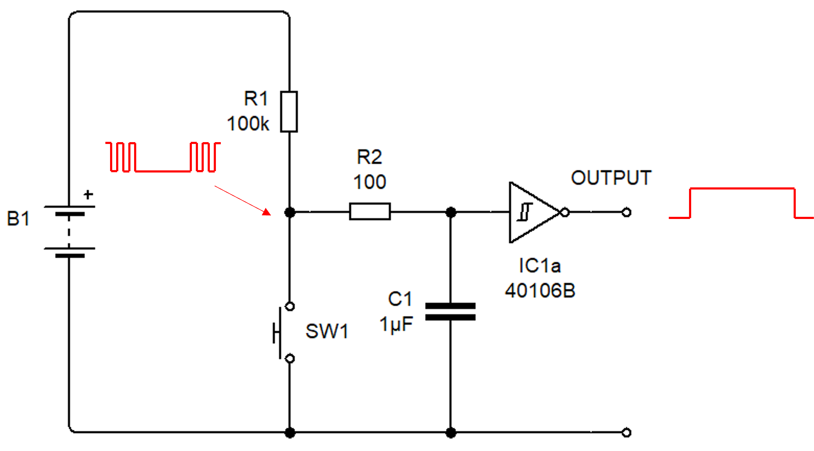
This circuit uses a Schmitt inverter as the active component in this debounce circuit.
Normally the capacitor holds a charge, placing a logic 1 level on the input of the inverter resulting in a logic 0 on its output.
When the switch is depressed the capacitor quickly discharges through R2 causing a logic 0 to appear at the input of the inverter and therefore a logic 1 at its output.
As the switch is released the capacitor charges up via R1 and R2 once again. Once the capacitor voltages reaches the threshold voltage for a logic 1 the inverter is triggered resulting in a logic 0 on its output.