Engineering & Technology
WWW.CLARVIS.CO.UK
WWW.CLARVIS.CO.UK
Circuit boards can be manufactured using a chemical etching process.
The chemicals used in PCB manufacture are not pleasant and can be quite dangerous. You must therefore always wear goggles, gloves and an apron to protect yourself and your clothes. Apart from being very caustic the chemicals used can turn your skin orange and it doesn’t wash off!
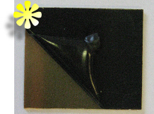
PCBs are made of laminations (layers) of different types of material. The diagram on the bottom right shows an exagerated cross section view of a brand new piece of PCB:
The fibreglass gives the PCB strength and is an insulator.
The copper layer is etched in a way to form the tracks of your PCB design.
The light sensitive layer is used to protect parts of the copper during the etching process.
The protective plastic film prevents the sensitive layer from becoming damaged by sunlight.

The process of making a PCB is outlined in twelve stages below.


1. Design the PCB on software such as Circuit Wizard

2. Print the PCB design onto transparency film.

3. Using a shear, cut the blank piece of PCB to size

4. Remove the protective sheet to expose the photosensitive layer beneath.
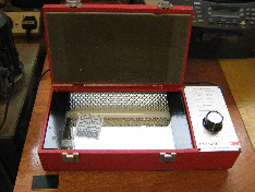
5.Place the transparency and board into the UV light box.

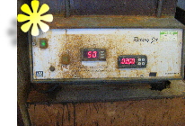
6. Close the lid and set the exposure timer to around 3 minutes.

7. Place the exposed board into the developer until the copper layer is visible.

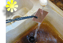
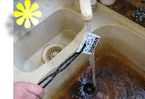
8. Wash the developer off the board with clean water.
9. Place the PCB into the etch tank.
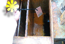
10. The exposed copper parts will etch away but the parts protected with the light sensitive layer will remain. This takes about 10 minutes.
11. Rinse the ferric chloride off the board with water
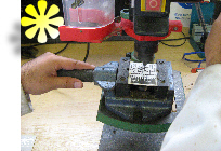
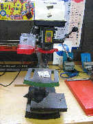
12. Once the PCB has dried, drill holes in the appropriate locations.